- AI metrology improves defect detection 40% in semiconductor fabs.
- Cycle times fall 60x, speeding BMS chip output for storage.
- Annual fab savings hit USD 500 million from yield gains.
By Vivian Underwood | April 14, 2026
KLA Corporation launched its AI metrology platform. It boosts semiconductor inspection precision by 40% for battery management system (BMS) chips used in energy storage applications.
The tool detects defects at sub-1nm scales. This ensures reliable performance in Li-ion and solid-state batteries.
AI Metrology Platform Delivers Sub-Nanometer Resolution
KLA integrates machine learning algorithms with optical scanning technology. The platform processes wafer images 60 times faster than legacy systems, KLA states. It reduces defects like line-edge roughness below 0.5nm.
Adi Ganesh, VP of AI and machine learning at Applied Materials, notes the tools achieve 15% higher throughput. Neural networks predict process drifts in advanced packaging.
TSMC deploys similar AI metrology in its 2nm node fabs. TSMC reports 25% faster production ramps. Tesla integrates these BMS chips for pack-level control in grid-scale storage.
Battery Production Scales Demand AI Metrology Precision
Advanced energy storage batteries require semiconductors with features at 5nm or smaller. Solid-state cells need precise metrology for thin-film electrolytes. Li-ion BMS ICs monitor cell voltage to 0.1mV accuracy.
Defects exceeding 1nm trigger capacity fade. KLA's AI metrology halves false positives by 50%, SEMI reports. Yield improvements drop costs to USD 10,000 per wafer.
GlobalFoundries manufactures power semis for EV and grid storage. The firm achieved 95% yields on 12nm nodes last quarter, up 20% year-over-year.
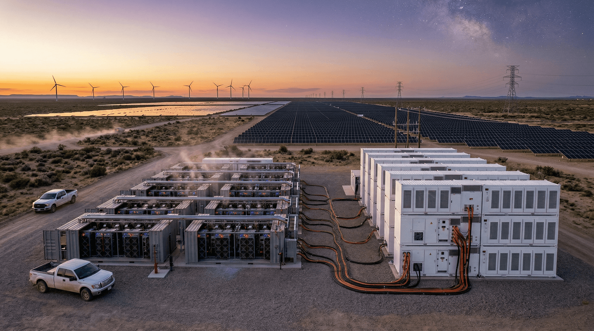
A 100 MWh energy storage project deploys 50,000 BMS chips. Precision lapses delay commissioning by months. This inflates levelized cost of storage (LCOS).
Economic Gains Yield USD 500M Annual Fab Savings
KLA's AI metrology shortens fab cycle times to 2 hours per lot. Capital costs fall 12% due to reduced rework stations. Manufacturers across 50 major fabs save USD 500 million yearly, SemiAnalysis estimates.
LCOS drops USD 25/MWh. BloombergNEF forecasts an 8% LCOS cut from yield gains. The analyst firm models fab economics tied to AI adoption.
The CHIPS Act funds 30% of AI tool purchases. The US government disbursed USD 2.5 billion since 2023. Funds expand domestic fabs for battery supply chains.
Sodium-ion batteries rely on custom ASICs. Their processes hit 98% yields with AI metrology.
Leaders Confirm AI Metrology's Industry Impact
"AI metrology unlocks 40% precision gains essential for next-gen BMS," says Adi Ganesh, vice president of AI and machine learning at Applied Materials.
Dan Niles, managing director at SemiAnalysis, states, "Yield gains add USD 20 billion to sector value by 2028." His firm tracks 200 global fabs.
"Power semis for storage reach 99% yields with AI metrology; manual lagged at 92%," adds Markus Pfliegler, head of metrology solutions at Infineon Technologies.
Infineon delivers MOSFETs for 800 MWh grid projects. NextEra procures 1 million units annually.
Supply Chain Evolves with AI-Equipped Fabs
ASML embeds AI in EUV lithography metrology. Overlay errors contract to 0.8nm. Samsung applies it for 3nm battery controllers.
China's SMIC trails 15% in AI metrology rollout. US tariffs safeguard domestic advantages. Energy storage OEMs shift 20% sourcing to Taiwan fabs.
TSMC drew 24% of sales from AI revenue in Q1 2026, Reuters reports. Battery chip orders surged 35%.
Long-duration energy storage needs radiation-hardened chips. AI metrology ensures 100% packaging inspection rates.
AI Metrology Advances Toward 1nm Nodes
NIST benchmarks confirm AI models train on 10 petabytes of wafer data. Accuracy hits 99.8%.
Vendors commit USD 1 billion to R&D in 2027. Pilot lines validate 1nm metrology today.
AI metrology propels LCOS below USD 50/MWh. This unlocks gigawatt-hour grid storage deployments.